[BUILD] New FET/RACK Official Help Thread - Please read first post!

GroupDIY Audio Forum

Help Support GroupDIY Audio Forum:

This site may earn a commission from merchant affiliate links, including eBay, Amazon, and others.
Hairball Audio said:
Guessing you have a side chain issue...too much compression maybe.  Go back several pages in this thread...look for the posts about measuring pad 22 and pad 21 at  all ratios.  I've gone through it a few times with people in this thread.

Pad 21
4    -1.83 VDC
8    -2.74 VDC
12  -3.83 VDC
20  -6.75 VDC

Pad 22
4    .8 VAC
8    1.7 VAC
12  2.2 VAC
20  2.5 VAC
 
Diamondj421 said:
Pad 21
4    -1.83 VDC
8    -2.74 VDC
12  -3.83 VDC
20  -6.75 VDC

Pad 22
4    .8 VAC
8    1.7 VAC
12  2.2 VAC
20  2.5 VAC

Pad 22 is hot as **** (level too high). That's the cause of the over compression you're seeing.

Double check all of your ratio PCB resistor values. Look for something like a 47K and 470Ω or similar mixed up on that PCB.

Mike
 
Hairball Audio said:
Pad 22 is hot as sh*t (level too high). That's the cause of the over compression you're seeing.

Double check all of your ratio PCB resistor values. Look for something like a 47K and 470Ω or similar mixed up on that PCB.

Mike

Everything is kosher as far as resistors. Maybe reflow the solder to the resistors and switches?
 
Hairball Audio said:
Check R78, R22, R36, R37.

Real close.

Ok. So everything seems fine with those. I cleaned up my P2P work and reflowed a bunch of my solder joints. I have lower values at Pad 22 but now can't get my output above 2.15VAC. Closer but still not 2.44VAC.

Pad 22
4 = .010VAC
8 = .014VAC
12 = .022VAC
20 = .036VAC

Thoughts?
 
Diamondj421 said:
Ok. So everything seems fine with those. I cleaned up my P2P work and reflowed a bunch of my solder joints. I have lower values at Pad 22 but now can't get my output above 2.15VAC. Closer but still not 2.44VAC.

Pad 22
4 = .010VAC
8 = .014VAC
12 = .022VAC
20 = .036VAC

Thoughts?

That's too low. You should be at around 0.065V AC @ 4:1 and 0.375 V AC @ 20:1 (roughly).

Have a look at the schematic:
http://mnats.net/files/fetrack/fet_rack_d_doc_v1.11.pdf

Pad 15 is the output of the first amp stage and is right before the output pot. You'd mentioned that was around 2 to 2.5V AC with a 0dB input and you controls midway with GR off. That seems good.

When you turn on GR,  pad 15 is connected to the side chain amp in the lower right half of the schematic.  That 2.5V AC at pad 15 flows through a series of resistors (depending on the ratio selected) on it's way to the start of the side chain amp which is pad 22. Even out of cal and the q bias set for max output, that pad 2.5 V AC at pad 15 will most likely drop to under a volt when switched to GR mode. That's some compression kicking in.

In 20:1 that lower voltage from pad 22 hits only R78 before it heads down to pad 22. That's where is should dip down to 0.375VAC (ish) across that resistor if I recall. The rest of the resistors in that string play a role as part of the voltage divider.

C17 blocks any DC and then R36 and R37 set conditions for Q7 (impedance/bias) that all effect your voltage. After the sidechain amp the voltage is converted to DC and sent back to the FET to apply GR.

My main point is that your having an issue between your 15 and 22 pads and mostly what's in that space is the ratio PCB.

Where on the PCB is your point to point work?

Remember we do flat rate repair on these.

Mike
 
Hairball Audio said:
That's too low. You should be at around 0.065V AC @ 4:1 and 0.375 V AC @ 20:1 (roughly).

Have a look at the schematic:
http://mnats.net/files/fetrack/fet_rack_d_doc_v1.11.pdf

Pad 15 is the output of the first amp stage and is right before the output pot. You'd mentioned that was around 2 to 2.5V AC with a 0dB input and you controls midway with GR off. That seems good.

When you turn on GR,  pad 15 is connected to the side chain amp in the lower right half of the schematic.  That 2.5V AC at pad 15 flows through a series of resistors (depending on the ratio selected) on it's way to the start of the side chain amp which is pad 22. Even out of cal and the q bias set for max output, that pad 2.5 V AC at pad 15 will most likely drop to under a volt when switched to GR mode. That's some compression kicking in.

In 20:1 that lower voltage from pad 22 hits only R78 before it heads down to pad 22. That's where is should dip down to 0.375VAC (ish) across that resistor if I recall. The rest of the resistors in that string play a role as part of the voltage divider.

C17 blocks any DC and then R36 and R37 set conditions for Q7 (impedance/bias) that all effect your voltage. After the sidechain amp the voltage is converted to DC and sent back to the FET to apply GR.

My main point is that your having an issue between your 15 and 22 pads and mostly what's in that space is the ratio PCB.

Where on the PCB is your point to point work?

Remember we do flat rate repair on these.

Mike

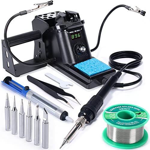
All this stuff is so cool! This post is like poetry to me. Haha. So here's the skinny. While trying to replace Q12 and Q13 so they matched, I also removed Q9 and Q10 to shuffle them around. All of these PCB points were mangled in removal. I don't know if I have a sh*t desoldering pump (it heats and pumps with the same unit) or if my patience is lacking but it was a mess.

I'll describe where each leg of the transistor has been reconnected. This will help me for comparing it to the schematic and maybe you could just confirm for me.

Q9
B - R43
C - Q10(B)/R47
E - R48

Q10
B - Q9(C)/R47
C - R51
E - C19 +

Q12
B - R66/Q11(S)
C - R67/R74
E - R44

Q13
B - R75
C - R74
E - P2/R69

I just checked these as I went along and don't see any issues. I'm  new to reading schematics though so I guess let me know if I missed something. If I had the dough I would've sent this in already. Times are a little tough right now so thanks so much for all of your help, Mike!
 
I opened up my other unit to compare since that unit works. It's v1.11 so I'm sure there are a few differences in the boards but right off the bat, I noticed that R13 and R36 on my older unit are 1M carbon film resistors and this new unit has 1M metal film resistors. I assume since they're the same value with different tolerances this shouldn't be a huge difference but I'm totally loss as to what else could be wrong at this point.

Also, R43 on my older unit has a 270k resistor vs v1.12 which has the 38.3k. This confuses me though because the schematic you gave me is for v1.11 and even that says 38.3k for R43 but again, that unit works. I have a few 270k and 38.3k resistors sitting around. Should I try switching those out?
 
Diamondj421 said:
I opened up my other unit to compare since that unit works. It's v1.11 so I'm sure there are a few differences in the boards but right off the bat, I noticed that R13 and R36 on my older unit are 1M carbon film resistors and this new unit has 1M metal film resistors. I assume since they're the same value with different tolerances this shouldn't be a huge difference but I'm totally loss as to what else could be wrong at this point.

Also, R43 on my older unit has a 270k resistor vs v1.12 which has the 38.3k. This confuses me though because the schematic you gave me is for v1.11 and even that says 38.3k for R43 but again, that unit works. I have a few 270k and 38.3k resistors sitting around. Should I try switching those out?

There are no major differences. In fact I think the only difference is that we removed the top pads from the input transformer footprint.

1M carbon/metal makes no difference.

R43 should be 38.3 on both.

Mike
 
Diamondj421 said:
All this stuff is so cool! This post is like poetry to me. Haha. So here's the skinny. While trying to replace Q12 and Q13 so they matched, I also removed Q9 and Q10 to shuffle them around. All of these PCB points were mangled in removal. I don't know if I have a sh*t desoldering pump (it heats and pumps with the same unit) or if my patience is lacking but it was a mess.

I'll describe where each leg of the transistor has been reconnected. This will help me for comparing it to the schematic and maybe you could just confirm for me.

Q9
B - R43
C - Q10(B)/R47
E - R48

Q10
B - Q9(C)/R47
C - R51
E - C19 +

Q12
B - R66/Q11(S)
C - R67/R74
E - R44

Q13
B - R75
C - R74
E - P2/R69

I just checked these as I went along and don't see any issues. I'm  new to reading schematics though so I guess let me know if I missed something. If I had the dough I would've sent this in already. Times are a little tough right now so thanks so much for all of your help, Mike!

Q9 B should have continuity to R43 and R44.
Q10  C should have continuity to R51 and Q8 C
Q10  E should have continuity to C19, R49, and E of Q7.

Look at the schem again.  Use your Ω tester to check connections.

Mike
 
SUCCESSSSSSSS!!!!!  I seriously cannot express the satisfaction that I'm feeling right now. The ratio buttons had WAYYYYYY too much solder on them. Or a bad solder job because when I removed the excess, everything began working. Thanks so much for all of your help, Mike! You're the man and these compressors are barnone.  Hopefully, I'll be grabbing a pair of Rev A's in the next few months!
 
Diamondj421 said:
SUCCESSSSSSSS!!!!!  I seriously cannot express the satisfaction that I'm feeling right now. The ratio buttons had WAYYYYYY too much solder on them. Or a bad solder job because when I removed the excess, everything began working. Thanks so much for all of your help, Mike! You're the man and these compressors are barnone.  Hopefully, I'll be grabbing a pair of Rev A's in the next few months!

Whoop! Enjoy.
 
Hairball Audio said:
Well everything seems to be working other than your GR meter.

If you don't have continuity between Q13's C and TP11...one of those pads is lifted off the trace.

Hey Mike! Thanks for the parts!

I have an interesting question, with new parts installed...I can get voltage on the "leg" of Q13 C, but not on the bottom side of the PCB.

Its like its putting out the correct voltage, but not making contact with the PCB, I think the pad is shot...can I hard wire to something?

Also, R71 DOES change the Voltage on Q13 C....man, I'm close and I can feel it!!
 
lackstudios said:
Hey Mike! Thanks for the parts!

I have an interesting question, with new parts installed...I can get voltage on the "leg" of Q13 C, but not on the bottom side of the PCB.

Its like its putting out the correct voltage, but not making contact with the PCB, I think the pad is shot...can I hard wire to something?

Also, R71 DOES change the Voltage on Q13 C....man, I'm close and I can feel it!!

Look at Q13 C on the schematic and look at the traces coming from it on the PCB. The collector of Q13 only attaches to Pin 2 of CN2 and TP11.  You should be able to use your Ω meter to look at the trace and confirm continuity.  If you have no continuity, the pad may be dead and you need to replace the trace with a bit of wire.

Mike
 
Hairball Audio said:
Look at Q13 C on the schematic and look at the traces coming from it on the PCB. The collector of Q13 only attaches to Pin 2 of CN2 and TP11.  You should be able to use your Ω meter to look at the trace and confirm continuity.  If you have no continuity, the pad may be dead and you need to replace the trace with a bit of wire.

Mike

PRAISE THE LORD IN HEAVEN!!!!!!

It's finally working! Man, that was a tough one....I had to connect a wire on the TOP side of the PCB,( Q13 C to TP11) no idea why...but who cares ;D
Thanks again Mike! I'm sure you'll be seeing more of me, hopefully just for more gear, not support  :D
 
Next set of questions. So I have both units calibrated properly but when running the same signal through both units, one is dramatically louder than the other. This is without the active link. With the active link turned on I barely get any signal out of the second unit regardless of which is set to send and receive. Any ideas?
 
lackstudios said:
PRAISE THE LORD IN HEAVEN!!!!!!

It's finally working! Man, that was a tough one....I had to connect a wire on the TOP side of the PCB,( Q13 C to TP11) no idea why...but who cares ;D
Thanks again Mike! I'm sure you'll be seeing more of me, hopefully just for more gear, not support  :D

Nice!
 
Diamondj421 said:
Next set of questions. So I have both units calibrated properly but when running the same signal through both units, one is dramatically louder than the other. This is without the active link. With the active link turned on I barely get any signal out of the second unit regardless of which is set to send and receive. Any ideas?

Surely a bad component value or bad solder joint somewhere. Start be determining if the difference is in the amp stages or the sidechain.  Is there a level difference between the two units if both are in GR OFF and the in/outs are set the same?

Mike
 

Latest posts

Back
Top