SSL "Talkback" Listen Compressor

GroupDIY Audio Forum

Help Support GroupDIY Audio Forum:

This site may earn a commission from merchant affiliate links, including eBay, Amazon, and others.
This way instead:

Redrawgain.jpg


Keith
 
Haha yes i redrew mine before you posted haha sorry...  Is that a better way to go? I don't understand your setup keith, only the simple ratio setup ala my picture
 
I guess they are essentially the same setup? except with the wiper at the input you can control both the feedback resistor and input resistor...
 
Well it means you can screw both sides of the gainset ratio at the same time, giving you more whack. Kindof like the difference between taking a baseball bat and only swinging forward as opposed to being able to haul out.
 
Haha nice. Okay well that sounds like a good way to go then. And much tweaking I bet - but the general setup seems okay now?  Any need for buffer capacitor such as 22pF on the OPA feedback leg too?

edit:  "Warning - while you were typing a new reply has been posted. You may wish to review your post. " - haha
 
Haha yeah  ;D

You might as well just go ahead and install it. You can always leave it out when you stuff.


Beautiful circuit I might add. Reminds me of a fancy Orange Squeezer...
 
Sure, sounds like a plan.  I'll add this cnb circuit to my layout as soon as I have the chance Lukas.

Aside from the CnB, I've got the layout setup with two relays: OMRON G5V-2-DC24 which should reverse the input txr when powered up.  Do you know if pin 1 is positive and pin 16 is ground on these relays?  That's the way I have them in the layout but I couldn't find any documentation on that really. I guess as long as there is a differential across pin 1 and pin 16? Ie could maybe ground 1 and put -Vdc to pin 16.
 
Oh yeah better check that twice. Relays are polar. I remember this seriously messed Stefan and me up one time working on the Q when need arose to mirror the entire master board, and all things were considered and no problem - EXCEPT the relays (that took an entire day to figure it out..."but I don't understand, we had it working...") Try to read THAT one out of a spectragraph ;)

Anyway, at this point, might I flag DANGER WILL ROBINSON. Let's take a step back and NOT slap everything onto a PC board together just yet, with all these ideas we are having you are heading for WORKING HELL.

Trust me on this one. You go through 20 or so entire new PC board designs and nuts in the process, especially when you have to keep making new entire boards when you decide to change something small.

What I'd suggest is this: Floating islands to begin with. Design the input and FET section down to C14 separately, the output section and detector separately, and let me send you a CnB board that's ready-made and tested. I can totally understand the itching to design the heck out of this bugger, but it's a lot easier in the workflow to get your function blocks made first, and then just needing to slap them together on a single board.

Sorry for the rant but I've been there.
 
Yah pin 1 should be +, that's tendentially the place + ends up...12V relays = good - you can run the logic circuit straight off a separate 18V PSU reg.
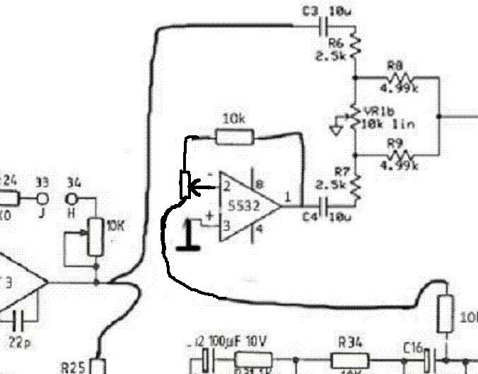
 
geetar_king said:
I guess they are essentially the same setup? except with the wiper at the input you can control both the feedback resistor and input resistor...

Too many questions to answer in a timely manner, so things are getting a little out of hand, but basically you HAVE to watch the load impedances on the preceding stages amongst other things. With your VR example the load impedance for the source to drive is down to 1,000Ω... which is asking a lot of some op-amps. 5534s whoucl be okay, but there's simply no reason to make it that hard on the poor thing, specially when there's a better way. -In addition, this way is inherently logarithmic in operation, whereas the scheme which you drew wolr dequire a special taper to 'feel' right.

Keith
 
Re GK: Nope - straight unbal all the way through to output, but no prob to bugger in a little SSM or THAT driver on the output - or yet even simpler just a balancing circuit a la GSSL - keeps with the SSL-style sound.

Oh but now haaaaang on a second - Why just last week I schemo'd that one Bal I/O with CnB all in 5532 flavor, even cross-coupled outputs, INTENTIONALLY for experimentation with compression elements. What a coincidence! Slated for layout and all (ok SMD but Eagle has a simple replace function).

And yeah, relay testing :)))) *click* - *drrrrrrrrrrrrrclickclick* - *drrrrrr*

Warning - while you were typing a new reply has been posted. You may wish to review your post.

Oh no, and yet again!

Warning - while you were typing a new reply has been posted. You may wish to review your post.

*donk*
 
Here:

Schematic

EDIT: sorry the one above is for later on - yes, the schemo you're talking about = 4 unbal ins and not quite sure what you mean by dual bridge?

One of the unbal ins on the dry line therefore would end up masquerading as T3 either way. Just need to watch out that the faze doesn't get reversibackwardsimixificated ;) - but actally that way it's straight because if you pull the signal the way you would in our previous photoshop orgy you'd end up cancelling everything out EXCEPT for the compression at the OPA's input.

Edit Edit: Ah thanks Keith, good to know my world wasn't entirely backwards as I marched into relays - somehow in that case I musta just stumbled over polar ones exclusively.

And Edit*3 yeah right with the tip of not forcing the opamps to work too hard if they don't need to, and good to know you can go down to 1K on 5532s if you want to...
 
R3/C1 and R49/C34 in bal. receivers are drawn wrong - they should both connect to positive inputs (pin.3) of corresponding opamps.
 
Well good morning TV! Thanks a heap for all those extra tips before - and for catching that one. I was still in Gyraf-Schematic-mode...

There we go, all better now  :D

oh btw ignore the pot divider R values in the cnb section
 

Latest posts

Back
Top