


MidnightArrakis
Well-known member
[Just Drill some holes and the rest can be excavated using a file or rasp] -- I just let a sheet-metal shop punch it out for me, along with all of the other holes and cutouts and inserting the necessary PEM-hardware. Works excellently EVERYTIME!!!The IEC rectangular hole can be made very simple. Just Drill some holes and the rest can be excavated using a file or rasp. In aluminum, it just needs fifteen minutes to do so. You don't need a special instrument for all, just use own skills and your done with standard instruments which everyone has at home.
/
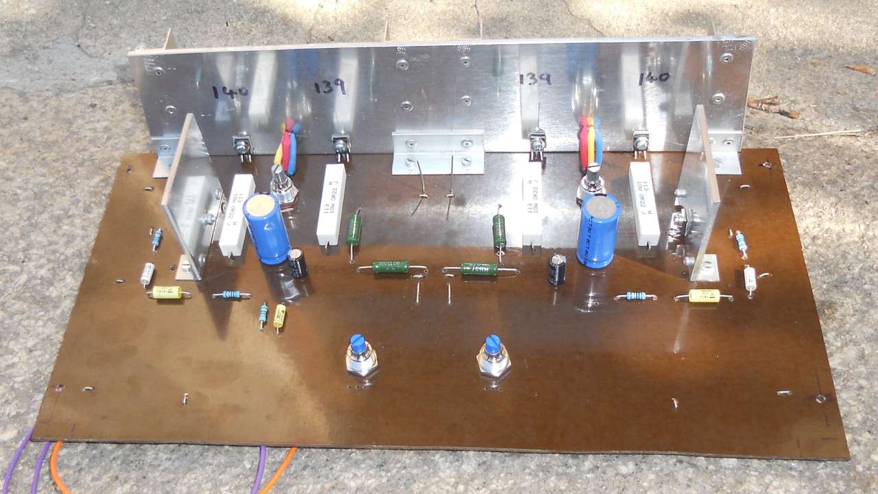
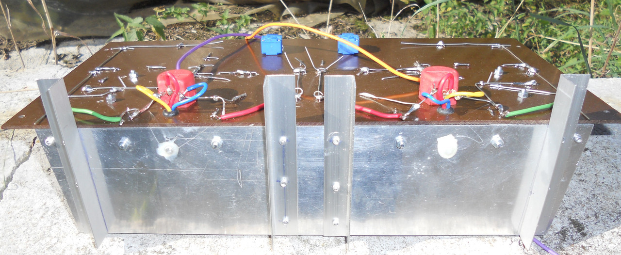
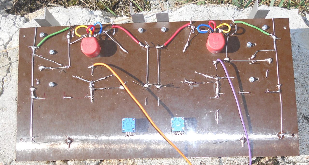


 no holes - so you "surface mounted" the components / bases ?